Difference between revisions of "Minimig Board v1.1 documentation"
Jump to navigation
Jump to search
(upd) |
(remaining issues) |
||
| Line 21: | Line 21: | ||
* The bottom silk screen has been cleaned up and added to the gerber file set. Minimig rev1.1 is 100% core and firmware compatible with the rev1.0 PCB. | * The bottom silk screen has been cleaned up and added to the gerber file set. Minimig rev1.1 is 100% core and firmware compatible with the rev1.0 PCB. | ||
| + | |||
| + | |||
| + | There are still issues remaining, see [[Minimig Board v1.0 issues]]. | ||
Revision as of 16:08, 26 August 2007
- The wire patch needed for rev1.0 to work is now incorporated into the layout. So, rev1.1 doesn't need a single wire patch.
Pin FPGA Name v1.0 Assignment v1.1 Assignment Comment 19 IO_7 User3 SPI_DOUT 79 IO_4/GCLK0 RAM_A15 RAM_A15 81 IO_4/DOUT SPI_DOUT NC
- Spare I/O (J9), User3 has been replaced with SPI_DOUT.
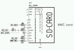
- SD/MMC: R49 has been decreased from 1000Ω to 100Ω for better MMC-Card compatibility.
 J11 - SD Card slot
- The PS/2 connectors are now properly connected to the frame ground.
- J5 - pin7,pin8,pin9 wired to "FRAME1"
- J8 - pin7,pin8,pin9 wired to "FRAME1"
- The bottom silk screen has been cleaned up and added to the gerber file set. Minimig rev1.1 is 100% core and firmware compatible with the rev1.0 PCB.
There are still issues remaining, see Minimig Board v1.0 issues.